

Profili:
Naučni profil Stručni profil
Struke:
Mikroelektronika inanoelektronika
Optoelektronika i laserska tehnika
Biomedicinski i ekološki inženjering
Aktivnosti:
Predavanja u okviruseminara katedre
Seminari Katedre
|
01.04.2011. 13:00 sala 104 Nenad Vukmirović Laboratorija za primenu računara u nauci, Institut za fiziku Beograd Organski elektronski materijali - simulacije elektronskih osobina i primene Organski poluprovodni materijali na bazi konjugovanih polimera ili malih molekula imaju velike mogućnosti primene za elektronske i optoelektronske naprave kao što su solarne ćelije, diode koje emituju svetlost i tranzistori. Glavni razlog tome je mogućnost njihove lake i jeftine proizvodnje. Da bi se razumeli procesi u ovim napravama, neophodno je poznavati prostornu i energetsku raspodelu elektronskih stanja u materijalu, kao i pokretljivost elektrona kroz materijal. Na ovom predavanju će biti dat pregled trenutne faze razvoja organskih materijala i naprava na bazi njih, kao i prikaz metoda kojim se elektronske osobine ovih materijala mogu predvideti i simulirati. Nenad Vukmirović je naučni saradnik u Laboratoriji za primenu računara u nauci u Institutu za fiziku u Beogradu. Osnovne studije je završio na Univerzitetu u Beogradu - na Fizičkom fakultetu (2003. godine) i Elektrotehničkom fakultetu (2004. godine). Doktorsku disertaciju "Physics of intraband quantum dot optoelectronic devices" odbranio je u avgustu 2007. godine na Univerzitetu u Lidsu u Velikoj britaniji. Od oktobra 2007-2010 je bio na postdoktorskom usavršnjavanju u Lorens Berkli Nacionalnoj Laboratoriji u Berkliju u SAD. Njegova istraživačka interesovanja uključuju teoriju i simulacije elektronske strukture i elektronskog transporta u poluprovodničkim neorganskim nanostrukturama, organskim materijalima i elektronskim i optoelektronskim napravama na bazi njih. Osvajač je zlatne medalje na 30. Međunarodnoj Olimpijadi iz fizike za srednje škole 1999. godine, a za naučni rad tokom doktorskih studija dobio je nekoliko prestižnih nagrada na nacionalnom i međunarodnom nivou: IEE Leslie H. Paddle Fellowship (za 2005/2006. i 2006/2007), IEEE Lasers and Electrooptics Society Graduate Student Fellowship (za 2006), kao i F. W. Carter nagradu za najbolju doktorsku tezu na fakultetu. Autor je 35 radova u vrhunskim međunarodnim časopisima (kategorija M21). |
|
|
06.10.2010. 11:00 sala 59 Marko Petrov, diplomirani inženjer-master Erasmus Mundus Master Program: Optika u nauci i tehnologiji U okviru predavanja biće predstavljena procedura prijave i uslovi koje studenti treba da zadovolje da bi konkurisali na Erasmus Mundus Master Program-e. Zatim, biće predstavljen OpSciTech program, način studiranja i kursevi koji čine ovaj program na Tehničkom univerzitetu u Delftu (Holandija) i Imperial College u Londonu (Velika Britanija). Biće prezentovani rezultati rada na optičkom dizajniranju trodimenzionalnih displeja postignuti na stručnoj praksi u okviru prve godine Master studija u Phillips Research centru (Eindhoven) u, kao i rezultati rada na realizaciji pasivnih mode-lock lasera na bazi optičkih vlakana ostvareni u toku izrade master teze. Marko Petrov, rođen je 1985. godine u Požarevcu. Nakon završene požarevačke gimnazije 2004. godine, upisao je Elektrotehnički fakultet Univerziteta u Beogradu i 2008. godine uporedo diplomirao na odsecima za Elektroniku i Fizičku elektroniku. Master studije u trajanju od 2 godine završio je u okviru Erasmus Mundus Master Program-a OpSciTech (Optics in Science and Technology) na Delft University of Technology, Delft, Holandija (prva godina) i Imperial College London, London, UK (druga godina). |
|
|
16.10.2009. 14:00 sala 104 Miloš Popović, MIT University of Colorado at Boulder (Boulder, Colorado, USA) and Massachusetts Institute of Technology (Cambridge, Massachusetts, USA) Silicon nanophotonics, optoelectronics and light-forces-based optomechanics for telecommunication and computing applications TNanophotonic circuits based on high index contrast (e.g. silicon or SiN) support strong confinement of light in wavelength-scale components and strong light-matter interaction. They raise the prospect of dense photonic integration on a chip, and of new device concepts with superior performance for applications in communication and computation. Major challenges to widespread assimilation of nanophotonics into mainstream technology are their enormous sensitivity, and limited scalability and complexity. I will describe work on strong-confinement nanophotonic devices that circumvent these challenges. First, I will address the design of dynamical nanophotonic devices, including switches and modulators, for high energy efficiency - a key requirement for chip-scale tunable optical add-drop multiplexers, future photonic on-chip interconnects for multi-core CPU and CPU-memory interfaces, and other emerging applications. Second, I will describe a new category of devices that merges silicon nanophotonics and nanomechanics into a new class of devices that makes use of light forces to cause nano-scale motion. In turn the motion changes the optical properties thus creating feedback. I will describe some of the exciting new device concepts and design opportunities made possible in this new field of research, and their implications for solving some of the existing challenges of classical nanophotonics. About speaker: Milos Popovic is an Assistant Professor of Electrical, Computer and Energy Engineering at the University of Colorado, Boulder (USA), and Principal Investigator of the Nanophotonic Systems Laboratory. Previously, he was a postdoctoral associate and independent investigator at Massachusetts Institute of Technology (USA). His research interests include nano-optomechanics, energy-efficient nanophotonic circuits, nanoscale device design and photonic circuit theory. His graduate research demonstrated a number of firsts in nanophotonic circuits for telecom applications - including telecom- grade filters, polarization transparency, and true-hitless switching. He is author or co-author of 15 patents and 60 papers, a member of the IEEE and OSA, and serves in peer review for several optics journals and conference technical committees. For more information, see: http://ecee.colorado.edu/~popovicm/ |
|
|
26.02.2009. 11:00 sala 104 Gaetano Scamarcio CNR-INFM Regional Laboratory on Laser Innovation Technology Transfer and Training - LIT 3 Research and development activities in optoelectronics and laser material processing at LIT3 The mission of LIT3 is to strengthen the Italian research activity in the field of advanced laser sources and related technologies. In the next five years the research focus will be kept on:
|
 |
|
27.06.2008. 11:00 sala 61 Dr Miloš Popović Optics & Quantum Electronics Group MIT, Cambridge, MA USA Integrated nanophotonics, optoelectronics and optomechanics: from telecom-grade wavelength routers to light-powered nanomachines Nanophotonic circuits based on high index contrast (e.g. silicon or SiN) support strong confinement (SC) of light in wavelength-scale waveguides and resonators with long photon lifetimes and strong light-matter interaction. They raise the prospect of dense photonic integration on a chip, and of new device concepts with superior performance. Nanophotonics has potential to revolutionize current technology in communication, computation and energy conversion, e.g. by harnessing large optical bandwidth, high energy-efficiency circuits, and all-optical feedback control. The challenge to widespread assimilation of SC nanophotonics into mainstream technology is their enormous sensitivity, and limited scalability and complexity. In this talk, I first describe SC nanophotonic devices based on solutions to the atomic-scale ultrasensitivity and scalability challenges. Microring-resonator-based nanophotonic circuits with telecom-grade performance are demonstrated leading to chipscale tunable optical add-drop multiplexers, a key enabling component for ultrahighbandwidth agile optical networks and interconnects. I also discuss a number of new device concepts including: dispersionless wavelength switches, polarization transparency, loop-coupled cavities, and low-loss open-system Bloch waves. In the second part of the talk, I will introduce recently proposed light-powered nanomachines and all-optical self-adaptive optomechanical circuits that rely on the interplay of resonantly-enhanced optical forces and the manipulation of optical resonances by mechanical degrees of freedom in nanophotonic structures. This new class of devices facilitates resonantly tailored optomechanical potentials, enabling picometerprecision positional control of nanomechanical structures and all-optically self-aligning microcavities that track the wavelength of an incident laser. These concepts lay the foundation for a fundamentally new class of nanophotonic devices with unique capabilities and numerous applications. |
 |
|
08.05.2008. 13:00 sala 104 Goran Isić Doktorant Univerziteta u Lidsu, Engleska Optimizacija poluprovodničkog spinskog filtra Spintronika je jedna od disciplina orijentisanih ka primeni kvantnih svojstava nosilaca i elektromagnetnog polja u čvrstotelnim nanostrukturama, na sličan način kao i (nano)fotonika, plazmonika, fononika i polaritonika. Konkretno, u slučaju spintronike akcenat je na eksploataciji spinskog svojstva elektrona koje je tesno povezano sa magnetizmom. Primeri spintroničkih komponenti koje danas postoje obuhvataju hard disk read heads zasnovane na giant magnetoresistance efektu, magnetske RAM memorije i racetrack memorije u kojima se informacije upisuju u magnetne nanožice upotrebom spinski polarizovane struje i koje su eksperimentalno realizavane u IBMovim laboratorijama početkom ove godine. Ove komponente su realizovane na bazi magnetskih materijala u kojima problem velike koncentracije nosilaca onemogućava procesiranje informacija pa se moraju sprezati sa poluprovodničkim komponentama pri čemu se javljaju veliki problemi zbog nekompaktibilnosti ovih materijala. |
|
|
22.06.2006. 14:00 sala 104 Dr Bojan Bošković Department of Materials Science and Metallurgy, University of Cambridge, England KARBONSKE NANOTUBE : SINTEZA I PRIMENE Karbonske nanotube su svojim fascinantnim fizičkim i hemiskim osobinama privukle i nastavljaju da spajaju istraživače na univerzitetima i u industriji iz do sada razdvojenih disciplina hemije, fizike, elektrotehnike, mašinstva i biologije u jedinstvenu novu disciplinu koja se zove nanotehnologija. Nanotehnologija se bavi materijalima i sistemima čije su dimenzije ispod 100 nm i karbonske nanotube su jedan od najznačajnijih nanotehnoloških materijala. Kratak pregled osobina, primena i sinteze karbonskih nanotuba će biti predstavljen. Rezultati SEM, TEM i Raman analize karbonskih nanotuba sintetisanih na niskim temperaturama koristeći radio frekventnu, mikrotalasnu i DC plazmu biće upoređeni sa rezultatima analize karbonskih nanotuba dobijenih klasičnom CVD metodom na višim temperaturama. Najnovija metoda trodimenzionalnog rasta karbonskih nanotuba za MEMS primene razvijena u saradnji University of Cambridge-a i MIT-a biće prezentovana. Novi kompozitni materijal sa karbonskim nanotubama u matrici karbonskih fibera i njegove potencijalne primene biće takođe prezentovane. |
|
|
11.01.2007. 13:00 sala 61 Chris P. Search Department of Physics and Engineering Physics, Stevens Institute of Technology, Hoboken, NJ 07030 Spin Current from Quantum Dots Embedded in a Microcavity Experiments on self-assembled quantum dots have recently resulted in electrical control of the charge state of dots embedded in microcavities as well as studies of the conductance and shot noise through these structures. At the same time, a number of experiments have shown strong coupling to a single optical microcavity mode. This work has motivated us to study theoretically how electrical transport through a quantum dot would be effected by coupling to a cavity mode. We have developed a model for quantum dots coupled to doped leads at zero bias with one of the Zeeman states lying below the Fermi level of the leads and the other above. Raman transitions involving a pump laser and a quantized cavity mode induce spin flips inside the dot that result in a pure spin current flowing from the dot. We have studied the characteristics of the spin current generated by this quantum dot spin battery for the case where (i) a spin flip is associated with emission of a photon into the cavity mode and absorption from the pump (ii) the spin flip is caused by absorption of a photon from the cavity and emission into the pump. In the former case, we calculate the spin current and the photon current associated with the photons leaking out of the cavity as well as the associated shot noise. We find that in our system, the spin current can be significantly larger than for the case of spin flips induced by classical driving fields. The frequency dependent current shot noise show dips and peaks that are a result of the discrete nature of photons. In the latter case, we find that the cavity mode and the spin current exhibit bistability as a function of the laser amplitude, which is driving the cavity mode. |
|
|
28.12.2006. 13:00 sala 61 Dr Zoran Ristovski International Laboratory for Air Quality and Health (ILAQH), Queensland University of Technology (QUT), Brisbane, Australia Atmospheric Nanoparticle Research: View from Down Under Nanoparticles are loosely defined as particles with diameters in the range of ~1 nm to 50 or 100 nm. While they are bigger than air molecule (0.3 nm) they are much smaller than the upper limits regulated by ambient air quality standards of 10,000nm (PM10). Due to their small size they do not contribute large quantities to PM10 mass but they dominate the number concentration and most of its surface area. Nanoparticles are often considered to be deleterious when they are inhaled or ingested into the human body. They penetrate deeply into the lung, where their large numbers overwhelm defensive mechanisms. They can induce structural changes to lung tissue; promote sensitivity to allergens, and increases mortality. Besides having detrimental health effects, recently their importance and influence on the global climate has been realised. Bursts of nanometer-sized particles formed from nucleated atmospheric gases and grown to detectable sizes (i.e. nucleation events) have been observed at coastal and marine environments around the world. Such nanoparticles can grow into larger sizes, being able to scatter incoming radiation and contribute a direct and an indirect (via clouds) cooling effect to the Earth's radiation This presentation will discuss the latest research trends on atmospheric nanoparticles conducted at the ILAQH, QUT Brisbane, Australia. |
 |
|
22.06.2006. 14:00 sala 104 Dr Bojan Bošković Department of Materials Science and Metallurgy, University of Cambridge, England KARBONSKE NANOTUBE : SINTEZA I PRIMENE Karbonske nanotube su svojim fascinantnim fizičkim i hemiskim osobinama privukle i nastavljaju da spajaju istraživače na univerzitetima i u industriji iz do sada razdvojenih disciplina hemije, fizike, elektrotehnike, mašinstva i biologije u jedinstvenu novu disciplinu koja se zove nanotehnologija. Nanotehnologija se bavi materijalima i sistemima čije su dimenzije ispod 100 nm i karbonske nanotube su jedan od najznačajnijih nanotehnoloških materijala. Kratak pregled osobina, primena i sinteze karbonskih nanotuba će biti predstavljen. Rezultati SEM, TEM i Raman analize karbonskih nanotuba sintetisanih na niskim temperaturama koristeći radio frekventnu, mikrotalasnu i DC plazmu biće upoređeni sa rezultatima analize karbonskih nanotuba dobijenih klasičnom CVD metodom na višim temperaturama. Najnovija metoda trodimenzionalnog rasta karbonskih nanotuba za MEMS primene razvijena u saradnji University of Cambridge-a i MIT-a biće prezentovana. Novi kompozitni materijal sa karbonskim nanotubama u matrici karbonskih fibera i njegove potencijalne primene biće takođe prezentovane. |
|
|
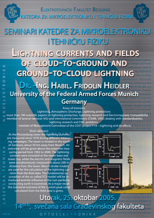
25.10.2005. 14:00 Svečana sala Građevinskog fakulteta Dr.-Ing. Habil. Fridolin Heidler University of the Federal Armed Forces Munich, Germany LIGHTNING CURRENTS AND FIELDS OF CLOUD-TO-GROUND AND GROUND-TO-CLOUD LIGHTNING Short abstract: At the Peissenberg tower the lightning currents are measured since 1978 during different measuring campaigns. The tower is located in the south of Germany about 50 km away from Munich. An overview will be given about the extensive measuring period from 1992 to 2000. The lightning currents were recorded at the tower base and tower top, while the electric and magnetic fields were simultaneously measured in about 200 m distance from the tower. Return stroke models are used for the calculation of the lightning currents from the field data. The fundamental assumption of the so-called TCS-model will be introduced and the influence of the non-perfectly conducting earth is examined. As a major result the statistical outcome of the current peak value calculated from the field data is given. |
 |